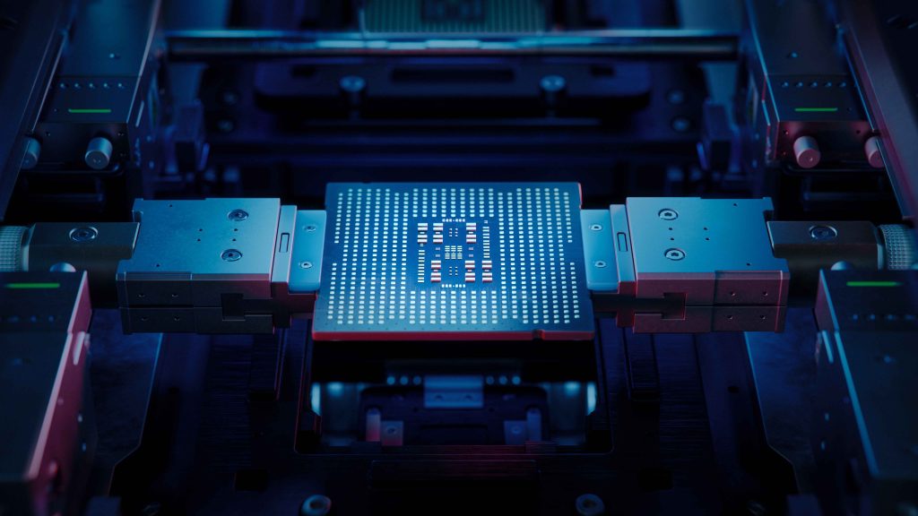
Process stability and yield
Laser sources for the semiconductor market
Semiconductor process expertise
Luxinar laser sources support wafer marking, wafer dicing, IC packaging, TGV processing and advanced packaging applications, with leading equipment manufacturers relying on them for wafer marking.
Flexible laser technologies
Luxinar offers nanosecond and femtosecond laser technologies with various wavelengths and pulse modes to address specific materials and process requirements in the semiconductor market.
A long-term partner for OEMs and integrators
Luxinar combines industrial laser technology with application expertise to help OEMs and system integrators develop, qualify, and scale reliable semiconductor manufacturing processes from concept through production.
Your challenges
How can semiconductor manufacturers improve process stability and yield?
By matching the laser source precisely to the material, process window and production target. Luxinar combines stable laser performance, controlled energy input and adjustable process parameters to support repeatable results in demanding semiconductor manufacturing environments.
Advanced packaging, heterogeneous integration, chiplet architecture and thinner wafers are creating new manufacturing requirements. Production workflows must deliver repeatable results while protecting high-value materials and supporting demanding production environments.
Luxinar addresses these requirements with:
- Reliable, repeatable processes: Stable laser performance supports consistent material interaction across demanding semiconductor production processes.
- Controlled energy input: Application-matched wavelengths and pulse durations enable precise processing of sensitive wafers, substrates and advanced materials.
- Productivity and process stability: A wide range of adjustable laser parameters, including power, wavelength, pulse duration and beam characteristics, allows manufacturers to optimize throughput, process quality and repeatability for specific production requirements.
- Expert application support: Luxinar works with OEMs and developers on feasibility studies, laser selection and customer-specific production optimization and application development.
Find the right laser source for advanced packaging and semiconductor manufacturing.
Why Luxinar
An industrial laser partner for semiconductor processes
Luxinar combines process knowledge, technology breadth and long-term support to help customers develop reliable laser-based manufacturing processes.
Application expertise
Luxinar helps customers evaluate the relationship between laser characteristics, material behavior and the required manufacturing result.
Reliable laser performance
Stable pulse delivery and controlled output support repeatable processing within demanding semiconductor process windows.
Technology breadth
Nanosecond and femtosecond technologies with different wavelength options enable application-specific laser selection.
Process-development support
Application specialists support feasibility evaluation, laser selection and customer-specific process development where appropriate.
Integration support
Luxinar supports OEMs and system integrators with laser-source integration, helping align laser performance, system requirements and application needs throughout development and qualification.
Long-term collaboration
Luxinar works with OEMs and system integrators from initial application discussions through process development, equipment integration and qualification toward production use.
Laser solutions for semiconductor market
Which semiconductor manufacturing processes can Luxinar support?
Advanced packaging, heterogeneous integration, chiplets, AI devices and compound semiconductors are creating new manufacturing requirements across the semiconductor industry. Manufacturers require laser technologies that deliver repeatable results, support process optimization and enable the processing of increasingly sensitive materials and complex structures.
Leading wafer marking equipment manufacturers rely on Luxinar laser sources in high-volume production environments, while OEMs and system integrators also use Luxinar technologies for laser debonding, wafer dicing, through-glass via processing, silicon carbide manufacturing and other semiconductor manufacturing processes.
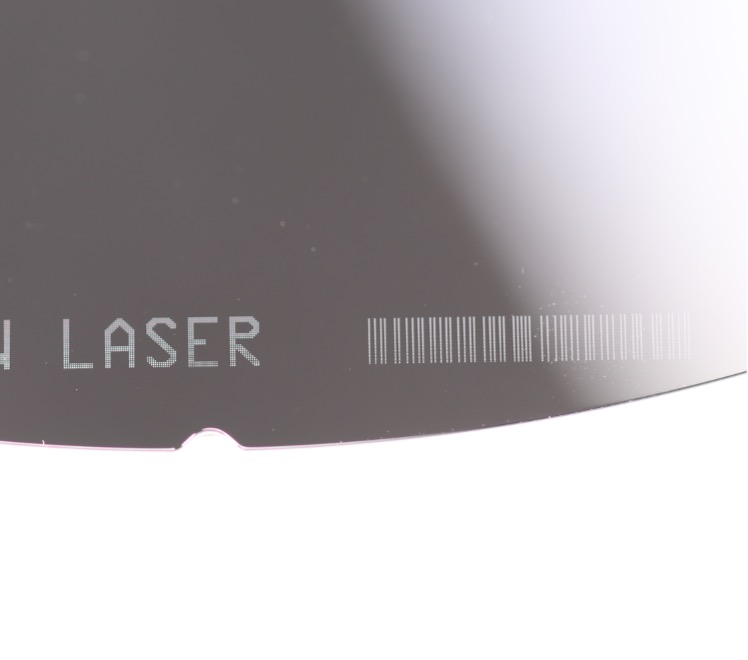
Wafer marking
Laser marking creates identification features on wafer surfaces within narrow geometrical and process tolerances. The process requires repeatable mark geometry and consistent performance across automated, high-volume production.
- Stable pulse-to-pulse performance
- High-speed operation for automated production
- Consistent marking quality across wafers
- Proven in high-volume manufacturing applications
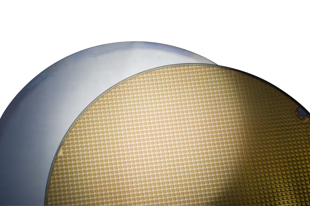
Laser debonding
Temporary bonding supports thin device wafers during demanding manufacturing steps in advanced packaging. Laser debonding technologies help separate carrier and device wafers while minimizing thermal and mechanical stress on sensitive structures. Luxinar supports equipment manufacturers and process developers with UV and infrared laser sources for glass-carried and silicon-carried debonding approaches, together with application expertise and process-development support.
- UV and infrared laser technologies available
- Supporting glass-carried and silicon-carried debonding approaches
- Configurable laser parameters for process optimization
- Application support from feasibility studies and process development through qualification
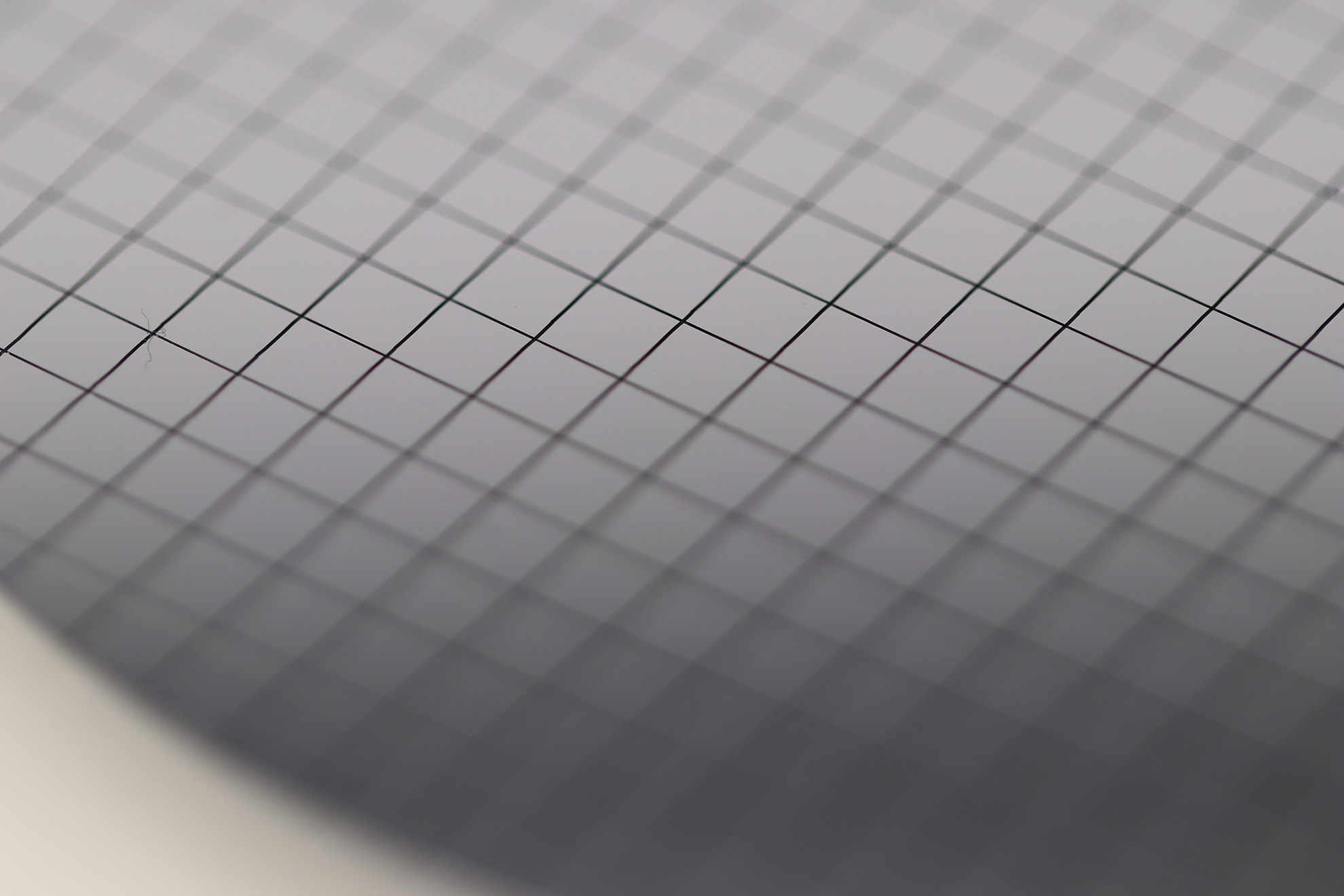
Wafer dicing
Laser dicing separates processed wafers into individual dies using either surface ablation or internal material modification. The required process outcome depends on the wafer material, die geometry, edge quality and production requirements.
- Ablative and stealth-dicing approaches
- Controlled energy deposition
- Flexible parameter optimization
- Suitable for advanced wafer materials
Through-glass via (TGV) processing
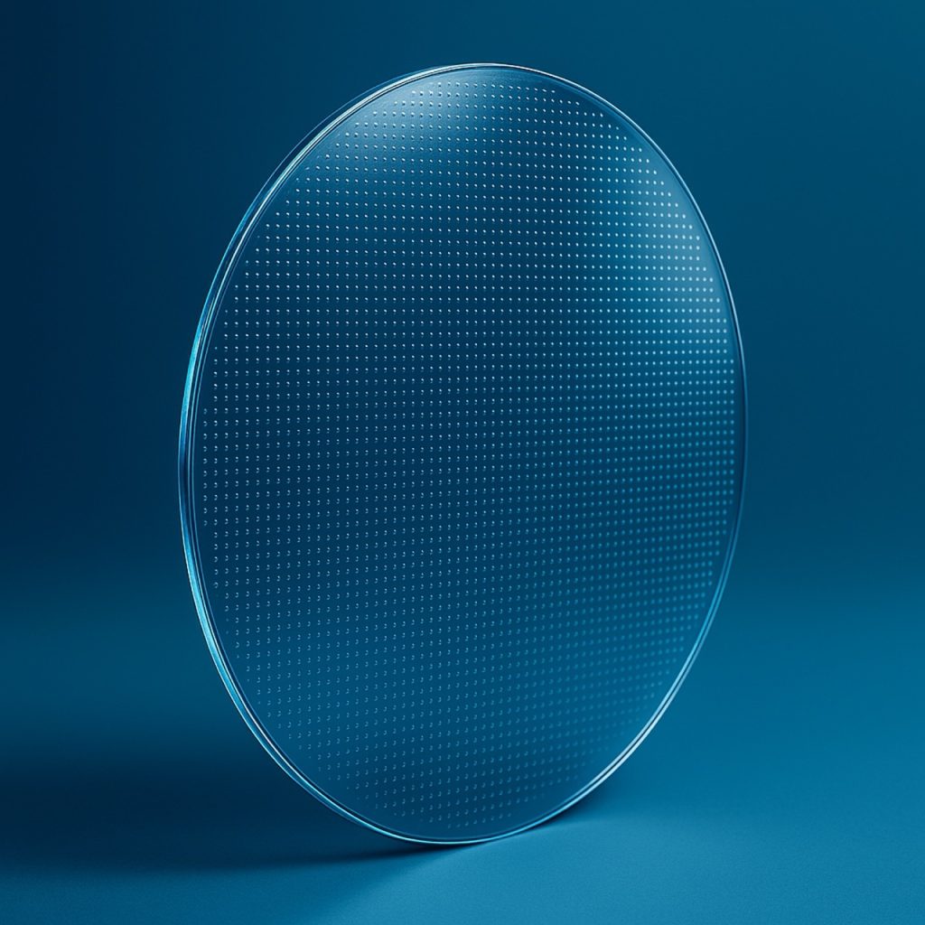
Through-glass vias provide vertical electrical connections in glass substrates and interposers used in advanced packaging applications. The process requires fine features, accurate hole positioning and repeatable via geometry at the required production speed.
- Fine-feature processing in glass
- High positioning accuracy through stable beam pointing
- Repeatable via geometry
- Process development support
Silicon carbide processing
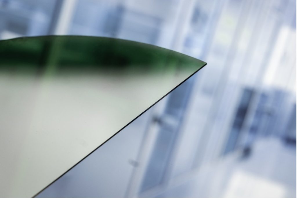
Silicon carbide combines high hardness with sensitivity to heat-affected zones, microcracking and chipping. Cutting, drilling and ablation processes therefore require controlled energy input to achieve the required quality while limiting material damage.
- Ultrashort-pulse lasers for contact-free SiC cutting, drilling and ablation capabilities
- Controlled energy input for reduced thermal impact
- Suitable for hard and brittle materials
- Process evaluation and optimization support
Advanced Packaging
Supporting the next generation of semiconductor packaging
Advanced packaging enables manufacturers to combine specialized dies, materials and functions within a single package. Technologies such as heterogeneous integration, 2.5D and 3D architecture, glass interposers and panel-level packaging are increasing the need for precise, repeatable manufacturing processes.
As advanced packaging evolves, there is growing convergence between semiconductor manufacturing, IC-substrate production and established PCB manufacturing approaches. This is creating new opportunities for technologies such as panel-level packaging and high-precision glass and substrate processing.
Luxinar supports equipment manufacturers and process developers in evaluating laser technologies for wafer processing, carrier separation, glass-via formation and difficult-to-process semiconductor materials.